1. Introduction.
What is it?
This is a very simple, but flexible design for a Flash ROM based ROMdrive card to suit an Apple ][,][+,//e,//gs.
The circuit is very simple, using only 3 chips (!!) and no other external components.
The software required to interface the card with Dos3.3 is remarkably simple (full source included) plus I am working on PRODOS support at the moment.
The Flash ROM chips are programmed in-system, so there is no need for any expensive complicated programming equipment. Consequently the design can be used to program Flash Roms for other purposes outside the Apple // environment.
There are 2 different circuit versions included in this archive:
one for a 28Fxxx version of the card, and another for a 29Fxxx version.
Different methods are required to program the 28Fxxx and 29Fxxx chips, but as far as reading the chips both circuits appear identical to the system.
Download the project archive
What are the files in this archive?
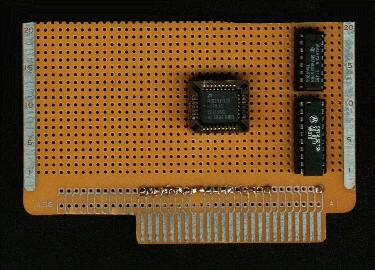
flashBOT.jpg
flashTOP.jpg
These are pictures of My 29f010 prototype, built on a standard Radio Shack experimenter board.
FLASHDISK.dsk
FLASHSOURCE.dsk
28fxxx.dsk
These are the disk images (in DOS sector order) that are referred to in the text. The 28Fxxx.dsk image contains some source code for programming a 28Fxxx version should you wish to build one.
I recommend using a 29Fxxx series chip, as it is much easier to program.
README.TXT
READ29F.TXT
Documentation files for the project.
ROMD28F.gif
ROMD29F.gif
Circuit diagrams for both the 28Fxxx and 29Fxxx version of the project.
Note: Power connections are not shown to the chips (+5v and GND) but you are expected to provide them. Refer to the relevent TTL and FLASH data sheets.
2. Theory of Operation.
The Flash ROM appears to the Apple ][ system as a number of 256 byte blocks that appear at $CN00-$CNFF, where N is the slot number the card is plugged into. The fact that the blocks happen to be sector sized simplifies DOS interfacing.
Several registers in the cards I/O space are also used.
(C0N0 space, where N = slot + 8. ie. C0A0-C0AF = slot2 space).
A reference to C0N0 will set the /OE pin on the flash ROM low, enabling the FlashROM in the CN00-CNFF space. A reference to C0N1 will set /OE high, disabling the chip for reading. /OE is set high during programming functions.
If you are using larger FlashRoms then you will have A16,A17 etc. connected.
These addresses are used to set the state of these pins:
C0N2 = A16 low
C0N3 = A16 high
C0N4 = A17 low
C0N5 = A17 high
etc.
A write into the C0Nx space will set the Address lines A8-A15 on the Flash chip.
For example : (assume a 29F010 card in slot 2)
LDA $C0A2; set A16 low on FlashROM.
LDA #$04
STA $C0A0; set high order address lines to 04 plus set /OE low for read.
Addresses $00400 - $004FF in the FlashROM now appear at $C200-$C2FF in the Apple ][ address space.
After power-on, or after a RESET block 00 automatically appears in the $CNXX space.
This occurs because the /RESET signal is applied to the 74LS259 and 74LS273 reset inputs, consequently /OE and any of the high address lines (A16 and up) are set low. Also A8-A15 are set to 0 by the reset on the LS273.
By simulating the ROM from a Disk ][ card in Bank 00 this ensures that the system will always see the card as a bootable disk drive card on power-up or Reset. It also means that you don't need a seperate EPROM to control the card's features.
3. Programming the chip.
Software is provided on the accompanying disk images for:
1. Erasing a previously programmed chip.
2. Programming a Flash chip from main memory
3. Reading the contents of a Flash chip into main memory.
4. Programming the Flash chip using DOS3.3's RWTS.
Full source code in BIG MAC format is provided.
The programming routines follow AMD's recommended algorithm, Intel chips use the same algorithm but I have not tested any chips other than AMD varieties.
Download the AMD 29F010 data sheet.
The Algorithms provided are for 28F256 chips (or 28F512 in two seperate blocks).
Sample code is also included to simulate a disk ][ controller ROM that loads in a DOS 3.3 image.
There is also code for programming the 29Fxxx variety chips and a DOS3.3 boot image, with instructions in a seperate doc file.
4. Summing up.
The programming algoritms are pretty obvious, so it should be easy to adapt them for bigger chips, or to program straight from large disk files or whatever.
Programming the chips is fairly simple procedure. I recommend you study the source code if you wish to see how it is accomplished, or if you want to adapt the design for another purpose.
I welcome questions of a technical nature, but strongly discourage questions like "What pin is Q0 on the '259?".
A certain knowledge of Hardware construction and also of 6502 assembly language is assumed in this project.
If you don't feel up to constructing it, DON'T!!